Design of LVCMOS output drivers poses significant challenges in integrated chips such as those involved in high-speed communication and low jitter clock generation. At higher speeds, dynamic power ∑ CVDD2f becomes an overhead. This article discusses an approach and architecture that optimizes power and leakage while maintaining optimal signal integrity under PVT variations, while driving capacitive loads.
Limitations of the Basic Push-Pull Pair
The core of a LVCMOS driver is a pair of complementary transistors (PMOS and NMOS) driving the output line. Simple push-pull stages offer speed but often suffer from poor impedance matching with the PCB trace, leading to reflections and poor SI.

Theory of Impedance Matching
To avoid reflections at the transmission line, pull-up and pull-down impedances have to be matched to Z0. The method adopted to measure this impedance makes the difference between optimal and sub-optimal designs especially for power. Reduction in capacitive load at the driver stage will have cascaded effects in power savings, since each preceding stage can be sized smaller.
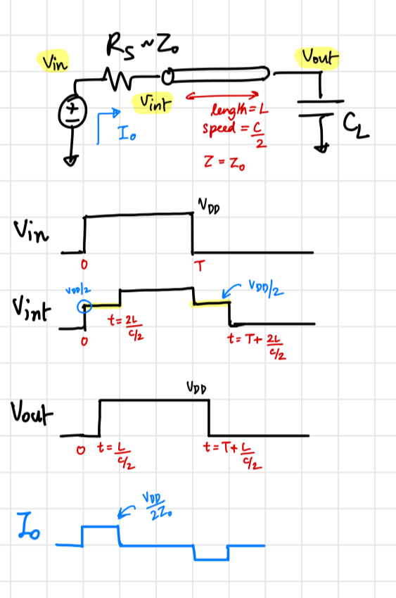
Shown in Figure 2 is the behaviour of the ideal impedance-matched LVCMOS driver driving a capacitive load through a trace. Since the looking-in impedance of the driver matches the trace, the voltage pulse amplitude gets divided by 2 at Vint node, according to the reflection formula. The reflected wave travels towards the capacitive load and gets completely reflected back at Vout towards the driver side.
Once the reflected wave reaches the driver side, it gets absorbed fully since the impedances match at node Vint, preventing any further reflections. This leads us to the design rule that the driver must be a circuit which can source and sink I=VDD/2Z0 while presenting an impedance of Z0 for a voltage range of VDD/2. This is the same as saying it's a resistance R=Z0 connected to supply during pull-up and to ground during pull-down.
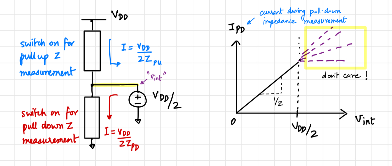
Impedance Measurement
As discussed above, the optimal voltage to measure pull-up and pull-down impedance is VDD/2. The current sinked and sourced at this voltage point provides a direct measurement of the output impedance Zout=VDD/2I.
Architectures
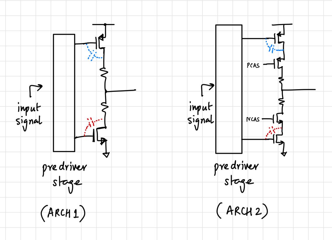
The basic architecture with impedance matching involves a push-pull pair with a resistor in series. Sizing the transistor large would give us a low Ron from it and it would be easier to bias it in the linear (triode) region by sizing the series resistor appropriately (R=Z0-Ron). This incurs a heavy penalty on pre-driver stage power and leakage due to the large transistor sizes. The optimal approach would be to extract as much of the resistance from the transistor while still maintaining it in triode. The impedance measurement method discussed here, helps us to do this.
Utilising HVT transistors as the switching elements cuts down leakage. Further, since the driver is an inverting stage, the gate capacitance that the pre-driver needs to drive will be very high because of Miller effect. A cascode transistor can be used to reduce the effective capacitance seen by the pre-driver (see ARCH2 in Figure 4). This also helps when the supply voltage range to support is too high for the HVT devices to support.
Careful design is needed to maintain both the transistors in triode with the right Ron across PVT and Monte Carlo variations. The contribution of each element towards the total impedance Z0 needs to be adjusted looking at tradeoffs of power and leakage.
Practical Considerations
Considering PVT variations and aging effects, process trimming would be required for maintaining controlled impedance. Slew rate control can also be implemented by staggered turning on of driver slices. Feedback based control of impedance is an option if variations due to temperature change need to be cancelled.